
A stop light with a devilish edge to it.
Background
Today’s LEDs are way to sexy to ignore. Just look at them, so tiny and so efficient, and the tech behind is getting better really quick now. I have to admit that the CREE XP-E LED itself was one of the main driving factors to begin this project in the first place. Let’s have a closer look:
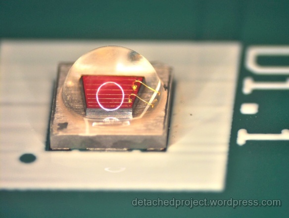
CREE XP-E2 – high power, SiC LED.
the XP-E2 series are some of the smallest footprint (3.5×3.5mm), high power LEDs out there. A tiny red XP-E2 will deliver, on average, 74lm at just 350mA and 2.2V(!) equaling to just about 100lm/W. Which, for red emission, is a pretty cutting-edge efficacy (at the time of writing).
Attached to some ceramic, high thermal conductivity carrier at the back and encapsulated with a round PDMS lens on top, here it is, a little devil. Anybody used to the more old-fashioned plastic-packaged LEDs can be surprised about the XPE’s lens shape as it, in essence, does not change the luminous intensity distribution of the approximately lambertian die emission. So the lens is in practice not more than a means of sealing the junction off from the environment while maximizing light extraction from the package by reducing reflections at the boundary with air.
It’s worth noticing that XP-E’s are very layout-friendly thanks to their electrically isolated heat-sinking pad running across the middle of the footprint:
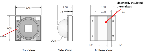
The same property also allows some improved heat evacuation solutions for instance, where all LEDs can have their thermal pad directly soldered onto an exposed core of a metal clad PCB (MCPCB) [How did those Sink-Pad guys manage to patent an idea this simple?].
Requirements
I didn’t have to wait long for a perfect occasion to utilize the mighty XP LED from CREE. It so happened that AGH racing team needed to build themselves an upgraded break light for their insane racing bolid. That made a perfect case not only to enable them to unleash some serious lumen output but to do so right along the clouds of burning rubber. That’s properly detached!
Taking into account the application and some little regulatory requirements the light had to have a minimum active surface of 15cm2 and be clearly visible in stark daylight…so we can forget using low power LEDs, and getting away without using optics, but what’s more important – the rules do not foresee any upper limit to the luminous intensity. In other words, a perfect case for a detached project.
Components
The optics
Owing to the popularity of their predecessors there exist dedicated optics designed for this LED range. Since we’re after a little bit of that F1 brake light appearance, the set of optics from LEDiL made a perfect addition to the project.
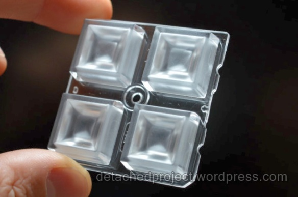
LEDiL LED optics array C12361_HB-2X2-W. One such array is 50mm x 50mm large.
It’s diffuse surface helped fulfill the apparent active surface requirements with just 8 LEDs (giving about 18cm2) while the 52o luminous intensity distribution (FWHM) allowed even higher energy density right behind the vehicle while still running decent “viewing angle”. It should be noted that the geometry of the optics is optimized for a white XP-G, however the red XP-E2 LED angular intensity distribution is very similar, according to the datasheet, so no significant optical loss should be introduced because of miss-coupling of the light into the optics.
The driver circuit
Power LED will demand some little power drive. In order not to squander the precious efficiency of the system and knowing we will be running off something like a car battery (10-14V), the obvious option is to equip the lamp with a DC-DC converter capable of driving 8 of our XP-E LEDs. There exist a huge pile of switch mode power ICs out there and on top of things each can often run many different topologies, so it’s usually hard to just pick one. A very useful resource for filtering out available switch mode ICs based on your requirements can be found at DCDCselector. We already are restricted by the possible supply voltage range, we would also like to have the current, rather than the voltage controlled in the loop and we know the LED count that needs to be driven. So with 2 parallel chains of 4 XP-E2 LED’s in series we will need 4×2.2V – about 8.8V – which is close to the car battery supply – and that just great since the closer we can get to the supply voltage, the easier it will be to use reasonably rated components for our DC-DC driver. In other words we end up with a buck-converter that will reduce the 10-14V input to about 8.8V output. Looking through various different ICs that could do the job I was really searching for one that would not demand too many components to make it a nice and simple design.
Electrical design
The driver
A DCDC IC from Texas Instruments – the lm3406, dedicated for step-down (buck), current mode applications and utilizing a 2A internal MOSFET switch, appeared to make an impressive work at reducing the count of the necessary external components. Below is the electrical schematic we are ending up with as a result of utilizing this IC:
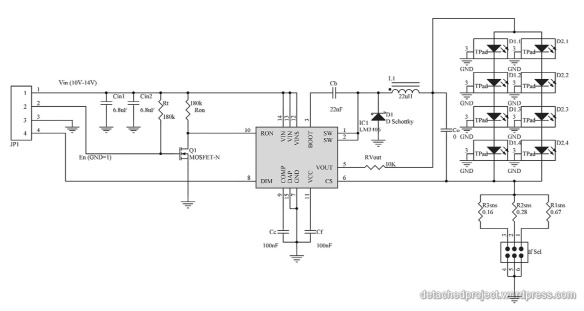
With an internal switching transistor all the LM3406 needs, beside the obvious inductance (L1), are input capacity (Cin1 and Cin2) to prevent EMI conduction down the supply wiring, a resistor to choose a suitable switching frequency (Ron) (or rather suitable on-time length in case of this specific IC, more explanation further), a Schottky diode (D1), a small precision resistor (Rsns) that will close the feedback loop to achieve regulated current through the LED array (in our case there are three Rsns resistors to have 3 luminous flux levels to choose from). If all is in specs (right components selected for the input levels and load requirements) one does not even need to use an output capacitor (C0). A couple more small caps are required just to ensure proper noise decoupling on the IC supply and reference voltages (Cf and Cc) and a bootstrap capacity (Cb) to help keep the internal MOSFET on throughout the high state, and that’s all.
It’s worth noting that, beside the obvious fact that it is a non-synchronous driver (a free-wheeling diode D1 present) , TI refers to it as “controlled on-time converter”. This generally means that we get to set the time the switch will be on (using R0n resistor). The IC will simply follow this required ON time with an OFF time necessary to achieve a duty cycle producing a steady state on the output. This means that the switching frequency is not really fixed in lm3406, but can slightly float about. This makes it a little different than a book case, fixed switching frequency converters, and may take getting used to but TI, as usual makes a great job at documenting all information necessary to design efficiently with this IC, right in the datasheet. All in all, once you can translate your ON time into a frequency, you can follow “by the book” which will converge with the approximate equations provided in the datasheet or use the precise equations with some “magic numbers” that are present at the end of the datasheet, providing extra levels of precision to your design process.
I will not be getting into the details on component values selection. Its all there, really well explained.
Note that the DIM input is also routed to the 4th pin of the connector so that dimming can be performed independently of the current selection by PWM.
lm3406 is dedicated for LED load and consequently it works in the current mode which means that the feedback loop will ensure proper functioning of the converter even without the C0 capacitor . So, one item less on the BOM list, just the way we like it.
Now, be not mistaken, this still is a properly detached project. Just because it has few components it does not mean it is cheap. The cost of the Cree XP-E2 LED is one thing but also the current control demands expensive, precision value current sense resistor Rsns, and we have three of them. Secondly, the buck topology has current ripple naturally occurring on the input side during switching. This demands large and stable capacity to be present across the input terminals of the converter to ensure it does not disrupt itself (stability) and other devices connected to the same power supply line or via EMI.
As a result the input capacitors Cin1, Cin2 will also be relatively expensive since they should have the X7R dielectric. Not just because the datasheet says so, but because we wouldn’t like the rated capacity to go down too much with the inevitable heat generated behind the vehicle by falling for a single, small Class 1, Y5V cap instead. A great resource to see how smd caps are made and how strongly different dielectrics affect capacity in changing electrical and environmental conditions can be found here. Note that there are 2 caps used in parallel to produce enough capacitance due to the necessity for considerable derating of this type (X7R, class 2 ceramic) under DC bias.
Components values
Lets say we would like the light to have 3 possible forward current levels:
If1=2*150mA
If2=2*300mA
If3=2*600mA
this translates into corresponding current sense resistors:
Rsns [Ohm] 0.29
Rsns [Ohm] 0.67
Rsns [Ohm] 0.16
To know the required components ratings we need to go over the worst-case scenario, that is the highest input voltage and the highest current setting:
Vin [V] 14
Vo [V] 9.2
Io [A] =If=IL 1.2
r [-] < 0.4 (current ripple ratio) [we will aim for 0.4 at nominal If2 current setting, therefore r will be smaller at higher current in a buck converter]
Vd [V] 0.5 (diode forward voltage)
Rswon [Ohm] 0.5 (switch resistance in ON state)
Vsw [V] 0.6 (voltage drop across the switch in ON state)
Δio [V] 0.48 (magnitude of the AC component of the current waveform)
D [-] 0.70 (duty cycle D ≈ Vo/Vin in a buck converter)
Id [A] 0.36 (average diode current Id≈ Io*(1-D) )
With these parameters we would get a maximum current waveform value < 1.7 A, which should not be an issue with the internal switch since, its average current is reduced proportionally to the duty cycle (Isw=Io*D). As far as the diode is concerned we could choose one as small as 0.5A but since we have lots of space on the board that is forced by the size of the optics, we can use a larger 1A, 500mW Schottky with the benefit of reduced forward voltage that will translate into higher electrical efficiency of the converter.
Last but not least we need to choose a suitable inductance. In this case the selection criterion is the current rating (min. 1.2A since Io=IL in buck) and saturation current (min 1.7A), as small DC resistance as feasible, and the availability of an inductance value most nearly matching the optimal efficiency. It is generally agreed that optimal efficiency is achieved when the converter is allowed to run a current ripple ratio of r=0.4. This should be the case for us at default input voltage (12.5V) and output current (700mA). Using the magic, precise equations given in the lm3406 datasheet we land ourselves with the following table of optimal inductance values:
| Ron [Ohm] | ton [s] | fsw [Hz] | L (optimal) [uH] (no output cap) |
| 820000 | 7.31E-06 | 1.03E+05 | 91.4 |
| 680000 | 6.09E-06 | 1.23E+05 | 76.2 |
| 560000 | 5.05E-06 | 1.49E+05 | 63.1 |
| 470000 | 4.27E-06 | 1.76E+05 | 53.3 |
| 390000 | 3.57E-06 | 2.10E+05 | 44.6 |
| 330000 | 3.05E-06 | 2.46E+05 | 38.1 |
| 270000 | 2.52E-06 | 2.97E+05 | 31.6 |
| 220000 | 2.09E-06 | 3.59E+05 | 26.1 |
| 180000 | 1.74E-06 | 4.31E+05 | 21.8 |
| 150000 | 1.48E-06 | 5.07E+05 | 18.5 |
| 120000 | 1.22E-06 | 6.16E+05 | 15.2 |
| 100000 | 1.05E-06 | 7.18E+05 | 13.1 |
| 82000 | 8.89E-07 | 8.45E+05 | 11.1 |
| 68000 | 7.67E-07 | 9.79E+05 | 9.6 |
| 56000 | 6.62E-07 | 1.13E+06 | 8.3 |
The line in red was my final choice that matched a decent WE-PD SMD Shielded Power Inductor of 22uH, from Wurth Electronic, offering RDC<1.5Ω, reasonable footprint and height.
PCB Layout
Starting with the optics geometry we end up with a simple 2x 2-by-2 array with 25.4mm pitch between the LEDs. Because the optics makes direct contact with the PCB everywhere around the LEDs, the driver electronics must be placed on the backside of the PCB. That’s just great since, for reliability we’d like to have decent area of copper spill around each LED. Because XP-Es heat sink pad is insulated we can generously copper spill the entire plane over that “dummy” potential (hence the LED schematic is equipped with a 3rd dummy, Tpad pin). At the flip side goes the driver.


With LEDs on one side and the driver on the other, the circuit is simple enough not to cause any layout problems. One should only pay attention to make the switching node potential (where L1, SW and D1 connect) track only just wide enough for the currents and to avoid running the sensing lines (connected to Vout and CS) parallel to it, to avoid any chance of instability in lm3406 output.
One problem encountered was the impossibility to use a proper through-hole automotive grade power connector. Illustrated below:

Altium’s DRC on a 3D model helps you spot collisions with non electrical components of the system as well.
It is in such cases that you feel all the effort of learning your ways in Altium pays off big time. The software is actually not only capable of generating an on-line 3D module of the PCB but also capable of DRC in 3D, which in this case immediately found the collision between the connector pins and the optics at the other side of the PCB. It’s obvious when you see it in 3D but working in 2D layout mode, on each PCB side separately, you could quite easily never notice this issue! Thumbs up to Altium since 3D integration of electronics and their complex packaging is going to play an increasing role in the future. This feature by then will be indispensable for everybody.
Here is the complete device model – being able to export the 3D model to a quite lightweight PDF is another great way to make prototype presentations.
TailLight_3D_Model_DetachedProjectV2
I really like the cross section view tool (available somewhere after right-clicking on the 3D render in the pdf file), pure engineer-ness. Altium supports output to STEP as well so mechanical engineers can have a bite as well.
The PCBs
The PCBs were realized using the prototyping offer of TechnoService. You can always count on these guys, and they did a great job at keeping tight tolerenaces on the NPTHs that register the optics. Very neat work indeed.
The PCB parameters were fixed to the prototyping service default’s, i.e. 1.55 mm thick FR4 (a little thick if you would ever wish to create efficient thermal vias) and 35μm thick copper layers (ok as entry-level thickness for power modules). The solder mask color was also fixed to the dark green default and this was less than optimal for the optically active PCB side. I decided to overcome the issue by designing a rectangular zone of white silkscreen layer around each LED component footprint definition resulting in an “emulated” white layer around the LED. This way some reflections from the PMMA optics could still be coupled back in instead of being completely absorbed by the green solder mask. Whether the silkscreen paint can withstand the thermal challenge of this solution – time will show (some white soldermaks often have issues standing up to the job resulting in very visible yellowing over time). To prevent light spill toward the back of the PCB and to keep the white silkscreen layer around the LED intact I decided not to introduce any thermal vias around the LEDs. This on one hand, because the application does not demand continuous work and because the prototyping PCB is quite thick, which renders thermal via’s not so efficient (unfortunately via-plugging with copper is not an option in a prototype either).
Assembly
I run the boards twice through a reflow oven. First attaching the LEDs, then turning the boards around onto a piece of epoxy board with holes where the LEDs were (to prevent LED contact with the oven tray) and solder all the driver components in a second reflow run. This is not ideal as not all LEDs may be so happy about re-entering the reflow profile. The XP-Es showed no sign of trouble though. In manufacturing, the LEDs would probably be attached in place with some epoxy glue right next to the solder paste and then all the components on the opposite side would be pick-and-placed, so that, a single reflow run could do the trick of soldering all components at once.
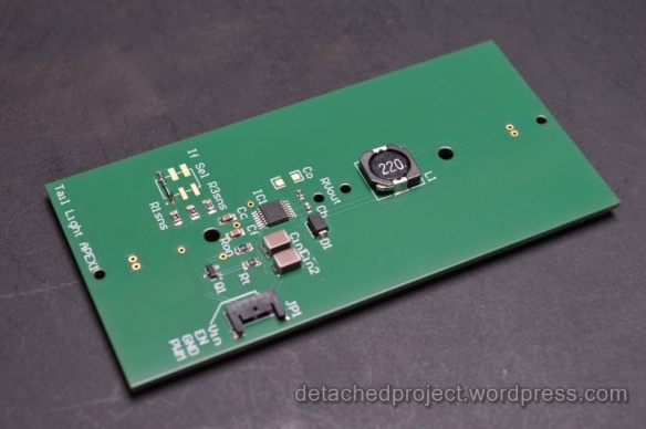
Driver side of the PCB.
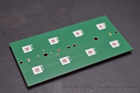
LED side of the PCB.
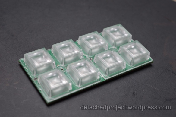
…with LEDiL optics.
Let there be…. Hell – Performance
Music please, suspense… we are about to start the lamp for the first time. Rising tension, nervous connecting of the wires… yes yes its going to be great…and power ON!!
It didn’t start up. No sign of life.
A short, critical look at all the components and 5 minutes later I found myself soldering the D1 the right way around. Apparently there was a mistake in the pin assignment of the diode component in Altium relative to the silkscreen layer cathode marking (To clear Altium of any suspicion, it was an add-on library component from somewhere way way back). (I fixed it for your guys in the silkscreen of the files attached at the end of the article, so no need for intervention). So second attempt…
It looked like this:

Switching modern power LEDs on without optics is a typicall “dont’t try this at home” thing (Image taken at 12.5V and 500mA supply).
The apartment filled with red light so much It literally sent my wife asking if everything was ok. I was expecting it to be bright, after all the luminous flux should be comparable to a 6W LED light bulb (of about 500 lm). The significant difference here is that all the radiant flux is emitted in a quite narrow, red wavelenght band, that makes it very, very intense indeed. What makes it really dangerous for your eyes is that the LEDs have such tiny emissive surface which makes for really high energy density (high radiance) and dangerous irradiance spots on your retina as a result. My eyes told me not to power it up without the optics anymore. You can take my word for it and not try it yourselves.
Seriously.
Installing the optics and setting the lamp up into the lowest current setting (If1), I was able to take a couple nicer shots:


Performance in numbers
Now, it looks good, but the question is- how good is it really?
Quick check across all current levels and all possible input voltages revealed no issues and a perfectly stable output. Also even if the input voltage goes below the design value of about 10V there the lamp just dimms out in a controlled fashion. Of course at If3 the board quickly gets quite hot. For the application you can still consider it to be ok (the light is on only when the brake pedal will be pressed, so for that short while the heat capacity of the system will do the job), however that level of current is not supposed to be injected into the LED junctions continuously. We would probably need a metal clad board (MCPCB) with thermal vias and a heatsink to ensure the LED junctions are at comfortable temperatures (<120*C) even in continuous operation. A quick check of the PWM input shows nice 10kHz dimming from as low as 20% duty cycle.
Below are the oscilloscope readings taken across the Rsns resistors and rescaled back into current at DC input:


The average currents indicated with the horizontal line are a little bit off compared to the initial assumptions due to the availability of specific Rsns resistors. The current ripple ratio at If2 of r=0.45 confirms that we are very close to the design work point though.
| Electrical*: | If1 | If2 | If3 | unit |
| Input voltage Vin | 9.3 to 14 | 10 to 14 | 10.5 to 14 | [V] |
| Input current: | 0.19 | 0.51 | 0.92 | [A] |
| Average LED matrix voltage: | 7.73 | 8.46 | 9.13 | [V] |
| Average LED matrix current: | 0.284 | 0.672 | 1.14 | [A] |
| Input el. power: | 2.4 | 6.4 | 11.5 | W |
| Output el. power: | 2.2 | 5.7 | 10.4 | W |
| Electrical efficiency: | 92 | 89 | 91 | [%] |
| Optical (including optics): * | If1 | if2 | If3 | unit |
| Approximate luminous flux: | 234 | 520 | 806 | [lm] |
| Approximate Efficacy: | 107 | 92 | 77 | [lm/W] |
*all relevant results obtained at Vin=12.5V
One interesting thing is that the electrical efficiency of the driver circuit is a little bit lower at If2 than the remaining current settings, which is surprising considering that the design was calculated for that particular output current. If anybody has a clue as to why that is, let me know in comments. Could it be that current ripple ratio r=0.4 is not a perfectly optimal assumption for lm3406?
The optical parameters are based on datasheet information of the LEDs and the LEDiL lens efficiency and not directly measured from lumen output so they should be considered as approximate values. However, radiating about 500lm of optical flux at just 0.5A, 12.5V input, which comes down to about 90 lm/W efficacy on a system level at If2, is a very very decent result indeed. Of course these numbers approximate real performance only when starting at room temperature and provided that the lamp is not on too long (in which case the LED junctions will inevitably run hotter and drop considerably in efficiency).
Take-aways
Components list:
| component | type | man. number | count |
| LED | Cree XP-E2 | XPEBRD-L1-0000-00801(by now worth to check out the latest XP-E device instead) | 8 |
| Lens array | Ledil 2×2 square | C12361_HB-2X2-W | 2 |
| Driver | LM3406HV-Q1 | LM3406HVQMHQ1 | 1 |
| Inductor | Wurth el. 22uH, 1.7A | 7447713220 | 1 |
| Diode | Schottky diode,1A | VS-10MQ060NTRPBF | 1 |
| Cin | Cin 6.8uF, 50V, X7R, 1812 | C4532X7R1H685M250KB | 1 |
| Cb | 22nF X7R, 25V, 0603 | VJ0603Y223KXXCBC | 1 |
| Cc, Cf | 100nF X7R, 25V, 0805 | VJ0805Y104MXXAC | 2 |
| Co | Co – none but foresee footprint 1206 | 1 | |
| Rsns1 | ~0.67Ohm 0.125W, 1% 0805 | ERJ-6RQFR68V | 1 |
| Rsns2 | ~0.28Ohm 0.25W, 1% 0805 | ERJ-6BQFR27V | 1 |
| Rsns3 | ~0.16Ohm 0.25W, 1% 0805 | 667-ERJ-S6SFR16V | 1 |
| Rout | 10kOhm (transient protection for Vout), 0603 | 71-CRCW0603-10K-E3 | 1 |
| Ron, Rt | 180kOhm, 1% sets the on time | 71-CRCW0805180KFKEA | 2 |
| Connector | Molex 4 way, 1.5A | 504050-0491 | 1 |
| En transistor | 2N7002, N-MOS Enchancment mode, 60V, 115mA | 512-2N7002 | 1 |
Design files:
Altium footprints, 3D component bodies and project files:
Followup
AGH Racing made their version of the lamp with some neat, in-house 3D printed housing to it. I was honored to see the lamp mounted in their racing vehicle throughout 2015 season. Here are some nice pictures featuring the race car and the brake light in action!


Many thanks to AGH Racing for their permission to reuse the images.

Looks like this lamp needs second live ! Let’s fix it
LikeLike